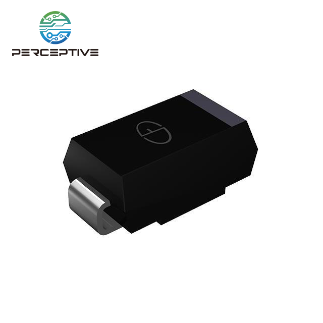
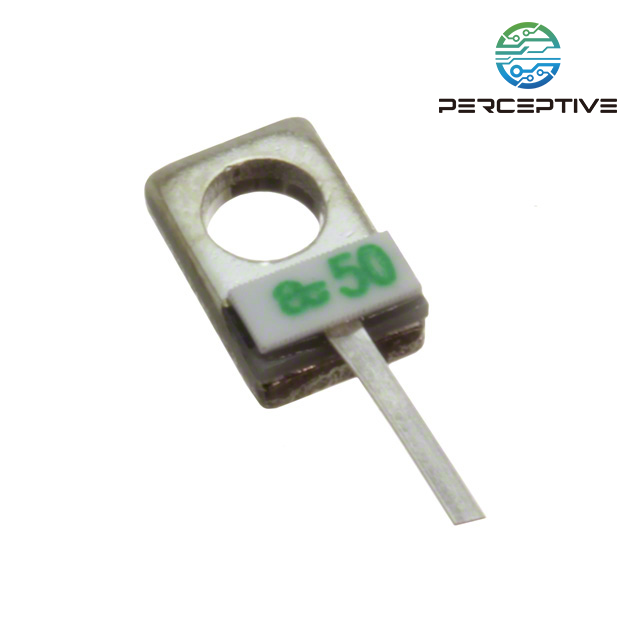
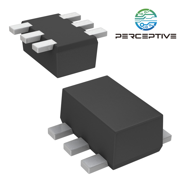
1. Small size perforated package - TO package (Transistor Outlines)
It is the earliest package type.
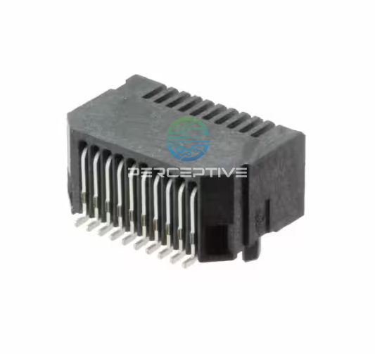
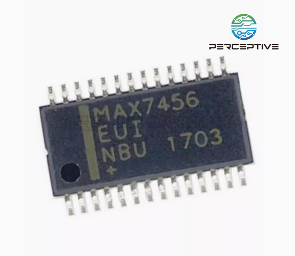
2. Leaded package with leads on opposite sides - SOP package (Small Outline Package)
One of the surface mount packages, the pins are led out from both sides of the package in a gull-wing shape (L-shape). There are two kinds of materials: plastic and ceramics. Features: the pins are distributed on both sides of the chip; it is very easy to weld; and it has high reliability, so it is the mainstream packaging type.
3. Double line perforated package - DIP package (Dual In-Line)
DIP packaging is adopted, and most small and medium-sized integrated circuits (ICs) adopt this packaging form. DIP packaged chips should be particularly careful when plugging and unplugging from the chip socket to avoid damage to the pins.
4. Four-sided leaded package - QFP package (Quad Flat Pack)
Plastic square flat package, when the chip has many functions and many pins, QFP package is generally used; so the pins of QFP are very dense and the reliability is high.
5. High ball count ball grid array package - BGA package (Ball Grid Array)
It has better heat dissipation and electrical performance; the pins cannot be seen, and the pins are all at the bottom. Once it appears, it becomes the best choice for high-density, high-performance, multi-pin packages such as CPUs and south/north bridge chips on the motherboard. Disadvantages: Difficult to weld.
6. QFN package (Quad Flat No-leads Package)
One of the surface mount packages, the four sides of the package are equipped with electrode contacts. Since there are no leads, the mounting area is smaller than that of QFP, and the height is lower than that of QFP; the materials are ceramic and plastic.
7. LCC package (Leadless Chip Carriers)
SMD package is designed for non-pin chip package, the pins are bent inward at the edge of the chip, close to the chip, which can reduce the installation volume. Disadvantages: troublesome debugging and welding.
8. PGA package (Pin Grid Array Package)
In the plug-in package, there are multiple square pins inside and outside the chip, and each square pin is arranged at a certain distance along the periphery of the chip. According to the number of pins, it can be surrounded by 2 to 5 circles. When installing, insert the chip into the dedicated PGA socket.
9.LGA package (Land Grid Array Package)
The contact display package is made with an array of flat electrode contacts on the bottom surface, inserted into the socket during assembly, and is used in high-speed logic LSI circuits.

