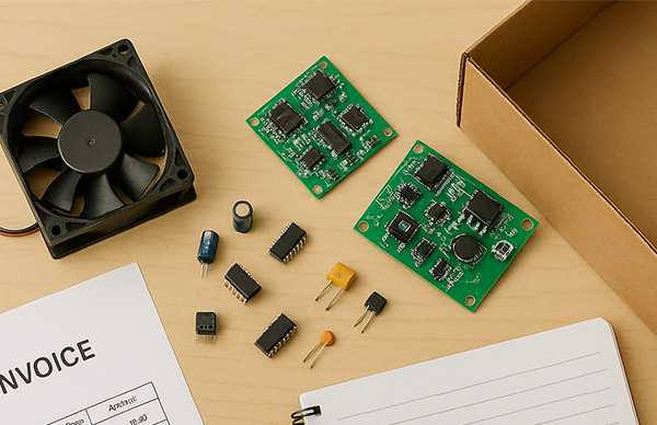
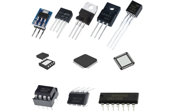
Sony IMX611, a direct time-of-flight (dToF) SPAD depth sensor for smartphones, can provide the industry's highest*1 photon detection efficiency, adopting single-photon avalanche diode (SPAD) pixel structure, can achieve up to 28% photon detection efficiency . This also results in lower power consumption for the overall system while enabling more accurate distance measurement of objects. The sensor also supports 3D space recognition, AR occlusion, motion capture/gesture recognition and other functions. In addition, the sensor integrates proprietary signal processing functions into the logic chip inside the sensor, which can reduce the post-processing load, thereby simplifying the overall system development and reducing system cost and time-to-market.

According to the company, the IMX611 uses a stacked configuration in which Cu-Cu connections are used to enable conduction of each pixel between a back-illuminated SPAD pixel chip (top) and a logic chip equipped with ranging processing circuits (bottom). These proprietary pixel structures combine to deliver the industry's highest photon detection efficiency of 28% when using a wavelength of 940 nm, which is commonly used in laser light sources for smartphones. This enables highly accurate identification and reduces overall system power consumption.
The company has incorporated proprietary signal processing into the logic chip inside the sensor to convert the RAW information acquired from the SPAD pixels into distance information output, all done inside the sensor. The sensor will bring opportunities to create new value for smartphones, including applications and functions that utilize distance information.
For more information, please visit the official website!